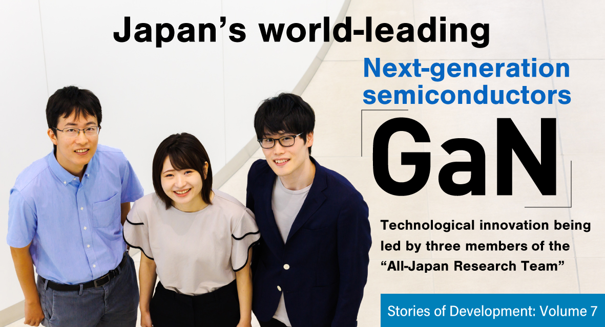
Three members of the ”All-Japan Research Team” are leading technological innovation in Japan’s world-leading next-generation ”GaN” semiconductors
-
GaN research is like “treasure hunting without a compass”
-
Withstand voltage resistance is 10 times that of silicon
-
Participating in national projects and focusing on “vertical” development
-
Application of GaN to electric vehicles
-
Ongoing trial-and-error at development sites
-
“Compared to Si design work, GaN is ......”
-
“Free and flexible research methods are like cooking”
GaN (gallium nitride) is attracting attention as a next-generation power semiconductor material. Fuji Electric is aiming to be the world leader by conducting R&D in national projects. We interviewed developers who are attempting to commercialize GaN power semiconductors through a process of trial and error.
GaN research is like “treasure hunting without a compass”

Power semiconductors are essential when using electricity. The application of power semiconductors is also expanding in the fields of electric vehicles and renewable energy. Si (silicon), which has long been the mainstream substrate material, is inexpensive, easy to process, and has stable quality. However, amid the trend toward decarbonization, the hurdles required of power semiconductors, such as energy conservation and miniaturization and weight reduction, have risen rapidly. Si is incapable of meeting many of these requirements.
Therefore, research and development of next-generation power semiconductor materials is underway. GaN is attracting attention as an emerging power semiconductor material, amidst the growing popularity of SiC (silicon carbide), a low-loss material that can withstand high currents and high voltages.
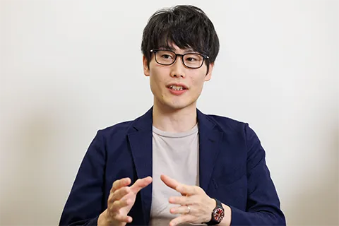
Mr. Kondo, who joined the company five years ago and is now in the Corporate R&D Headquarters, began his research on GaN when he was a student. In many respects, researchers still do not fully understand the nature of GaN, and therefore run into all kinds of challenges one after the other.
Mr. Kondo remarked, “There are still many unknowns, but diligent research provides a glimpse into its high potential. It’s like looking for treasure without a compass.” He continued by saying, “But this is why we want to continue our research so that we can maximize the potential of GaN.”
Withstand voltage resistance is 10 times that of silicon
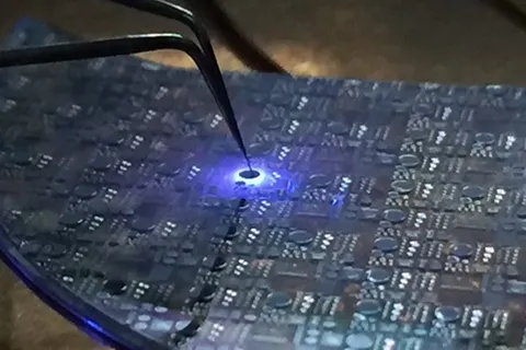
GaN is largely characterized by its “high withstand voltage” and “low loss.” GaN has 10 times the withstand voltage performance of Si and less than half the power loss of SiC. Therefore, it is expected to contribute to further miniaturization and energy savings in power semiconductors.
GaN research began to accelerate in 2014, when three Japanese researchers were awarded the Nobel Prize in Physics for the development of blue LEDs using GaN as a material. It just so happened that in the same year, Fuji Electric launched a national project to develop GaN power semiconductors in cooperation with substrate manufacturers, universities, and other research institutes to realize “vertical GaN-MOSFETs.”
Mr. Kondo, who was a university student at the time, recalls that “Many companies were already researching and commercializing light-emitting devices using GaN, but few were researching GaN as a power semiconductor. I got the impression that Fuji Electric’s research team was making great strides in their R&D efforts.”
Mr. Kondo remembers wanting to test the potential of GaN. This motivated him to join Fuji Electric.
Participating in national projects and focusing on “vertical” development
What exactly is a “vertical GaN-MOSFET”?
MOSFET is a type of electronic component (transistor) that has a switching function to turn current on and off. There are two types of transistor architectures: lateral, in which the current flows laterally, and vertical, in which the current flows vertically.
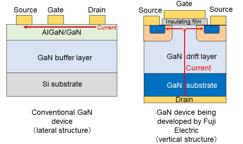
The lateral type is suitable for low withstand voltages and small currents, and is already being widely used in AC adapters for PCs and ultra-compact quick chargers for mobile phones. In contrast to the lateral type whose area must be widened laterally to increase withstand voltage, the vertical type can increase withstand voltage without changing the area and can handle large currents, making it suitable for use in larger power electronics equipment. However, the vertical type requires forming a power semiconductor device on a high-quality single-crystal substrate, as well as fabricating a structure through ion implantation (see Note), a process that is said to be impossible with GaN. For this reason, research did not proceed very well.
-
(Note)
-
This is a method of implanting impurities into semiconductor wafers by ionizing and accelerating them at high voltages.
In 2014, we started a national project to research vertical GaN-MOSFETs with substrate manufacturers, and this spurred development activities in a way that had not been possible before. The development of GaN power semiconductors has become increasingly important from the standpoint of economic security, especially since Japan has been involved in GaN research from the very beginning and holds many patents, enabling it to lead the world in this field.
Fuji Electric collaborated with Nobel Prize-winning scientist Hiroshi Amano, Professor at Nagoya University Graduate School, as well as many universities and research institutes in Japan, in an “all-Japan” development effort, and succeeded in demonstrating MOSFET device operation using ion implantation, an important technology for “vertical” type devices. This paved the way for the realization of GaN power devices.
Application of GaN to electric vehicles
GaN is suitable for moderate withstand voltages (600 V to 1.2 kV) such as those in EVs, and therefore is expected to be used as a power semiconductor in the power converters of electrically powered vehicles. The use of GaN offers important benefits, such as reducing the size of power converters, which increases the space inside the vehicle, and decreasing losses, which lengthens battery life and extends driving range.
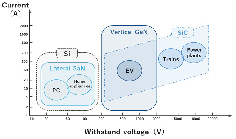
If GaN becomes mass-produced in the future, it is expected that it will be less expensive than SiC.
In 2019, Fuji Electric was the first company to successfully demonstrate the operation of GaN power semiconductors on a lab scale. The goal is to improve safety and cost, and to begin commercialization in 2030 or shortly thereafter.
Ongoing trial-and-error at development sites
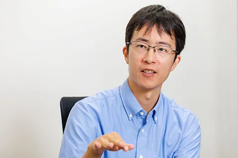
Fuji Electric is currently working on commercializing GaN power semiconductors through a process of trial and error. We spoke with some of the researchers who are at the heart of the development process.
Mr. Ouchi, who theoretically calculates and simulates the characteristics of semiconductors, said, “GaN and SiC have completely different properties.”
He further remarked, “The characteristics of semiconductors emerge when we create an oxide film on the surface of the wafer. It is relatively easy to create oxide films for Si and SiC, but when the surface of GaN is oxidized, it does not exhibit semiconductor characteristics.”
As a result, efforts are now being made through trial and error to bond an oxide film made of a different material onto GaN.
Mr. Ouchi continued to say, “It is very difficult to bond GaN and oxide film properly. Depending on the type of material and bonding method, the GaN surface can be oxidized instantly.”
“Compared to Si design work, GaN is ......”

Ms. Suganuma, who joined the development team for GaN power semiconductors in April of this year, had previously worked with Si in the Semiconductor Device Development Department at the Matsumoto Factory. She said that every time she evaluates GaN in her design work, she is surprised to see how many differences there are between GaN and Si.
She remarked, “Even when we make calculations to simulate the characteristics of GaN, we find that GaN does not produce the expected results. GaN research has really been an ongoing challenge.”
“Free and flexible research methods are like cooking”
However, GaN has the potential to become an important semiconductor material for use in power semiconductors. This is why these three talented people are proceeding with their research.
Mr. Ouchi said, “There are many things we don’t know about GaN, so we have a lot of freedom in research and development. Just like cooking, when you change the ingredients or rearrange the order of the recipes, you end up with something completely different. We are flexible in our thinking and try different ways of doing things.”
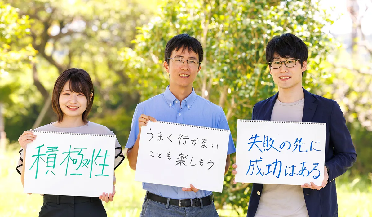
We asked the three developers to write brief messages for students (from left to right).
Ms. Suganuma wrote, “After joining a company, I think it is important to ‘actively’ gather information. Research positions require making presentations at academic conferences, so it’s important not to be afraid to take on new challenges.”
Mr. Ouchi noted, “In doing research and development, it is important to enjoy things even when they don’t work out well. Make it a goal not to dwell on problems, but to enjoy all parts of your work.”
Mr. Kondo remarked, “Failure is expected because we are still researching things nobody fully understands. I believe we can solve problems as long as we are willing to take on challenges and trust that ‘success lies beyond failure.’”
The three developers are gradually unlocking the mysteries. Fuji Electric’s continued research on GaN should play an important role in the worldwide race to innovate semiconductor technology.
Recommended

December 4,2025

July 30,2025

July 28,2025
July 7,2025
