Research & Development
R&D Projects
Analysis Technology
# Advanced Technology Laboratory # Fundamental and cutting-edge technologies
-
Three-dimensional characterization of an internal structure not visible from the surface
-
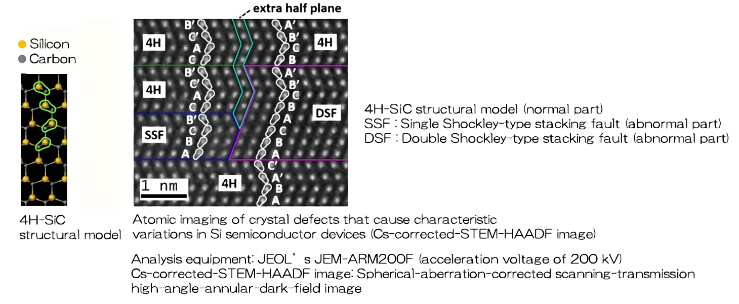
Clear observation of local structures on an atomic scale
-
Use of state-of-the-art analytical equipment within and outside the company
Analysis technology plays an essential role in improving a quality and a performance of products through a close cooperation with other research and development projects.
Products of cutting-edge technology such as semiconductor devices and magnetic storage media have been achieved by a precise control in terms both of the structure and the amount of constituents ranging from um to nm and from ppb to ppt, respectively.
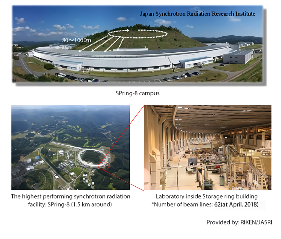
In order to accurately and quickly scrutinize atomic-scale phenomena in materials in various forms of bulk single-crystals, thin films, and interfaces, we utilize not only our own analysis equipment but also the most-advanced ones outside the company and the world’s leading synchrotron radiation facilities.
We extract intuitively easy-to-understand information from precisely measured data by advanced analysis with an aid of simulations, which helps engineers to get ideas at various stages of research and development.
-
*
-
µm is equivalent to one millionth of a meter, and nm to one billionth of a meter. ppb stands for "parts per billion" and ppt for "parts per trillion".
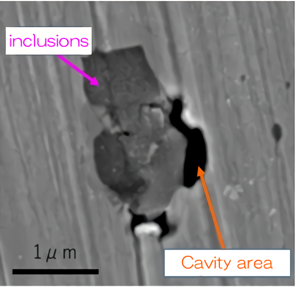
Ascertains the internal structure of corrosion areas
that cannot be detected from the surface
that cannot be detected from the surface

Stainless steel, SEM image of corrosion area
Atomic-scale analysis of defects
in SiC semiconductor devices
in SiC semiconductor devices

Challenges to reveal underlying mechanism with
most-advanced analysis equipment
(Large synchrotron radiation facility SPring-8)
most-advanced analysis equipment
(Large synchrotron radiation facility SPring-8)


![[Cross section]Continuous SEM images of cross section of corrosion area Movie](/about/technology/theme/__icsFiles/afieldfile/2023/10/31/analysis02_1.jpg)
![[3D image] 3D image of abnormalities (Orange: Cavity area; Pink: inclusions) Cavity volume: 7.5 μm3](/about/technology/theme/__icsFiles/afieldfile/2023/10/31/analysis01.jpg)