One Step Ahead! Fuji Electric's Fundamental Technologies
We provide an overview of our latest fundamental technologies that enhance our product development capabilities.
Materials Analysis Technology
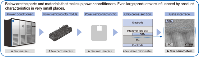
Analyzing phenomena that occur in minuscule places on a nano-level size to support manufacturing
Materials analysis is technology that uses equipment such as electron microscopes to investigate the causes of failures that occur in development and quality assurance, and to evaluate whether products are finished according to design. By effectively using the data we obtain from this analysis, we can improve product quality and shorten development time.
While there exist many products including power semiconductors for analysis, disk media, inverters, electromagnetic switches, and vending machines, the common point is that the properties of these products are affected at small places on molecular and atomic levels. For example, in the case of power conditioners equipped with SiC* power semiconductors, for energy-saving vending machines, the gate interface of the power semiconductor chip (the boundary of the SiC substrate and the oxide film) is a heat-insulating fiber hole (gap) in the vacuum insulation material that is needed to keep in heat. The size of each of the products is on a nano level (with a nanometer being one millionth of a millimeter), and as information on the product shapes and compositions can be obtained by irradiating them with electron beams and X-rays, we clarify the phenomenon that affects the products.
-
*
-
Silicon carbide
Alternative to silicon—the next generation of semiconductor material
Shortening the development period of SiC power semiconductor chips by leveraging the knowledge of the material
Analysis equipment: selecting the equipment from among more than twenty kinds is also a point of expertise.
The analysis group that performs material analysis is currently dedicated to proposal activities aimed at improving productivity, and its recent achievements include reductions in the number of prototypes for the SiC power semiconductor chips.
One of the important issues in the development of SiC power semiconductor chips is stable binding of the gate interface. There is a process in which an oxide film is formed on a substrate with a heat treatment, and when foreign objects are produced between the substrate and the oxide film, this has a major impact on switching (power on and off) performance. Certain elements can be added to eliminate the foreign objects, and there can be a great many combinations in the amount, timing, temperature, and other conditions in adding those elements.
This is where we created a test sample in cooperation with the development department, narrowing it down to a few kinds of combination patterns based on the phenomenon inferred from the material analysis. Using this sample, we were able to reduce the number of chip prototypes by 60% and shorten the development period. At the same time, we helped reduce the cost of creating prototypes, which uses expensive SiC substrates.
Voices of developers
Analysis Group, Applied Physics Research Department, Basic Technology Research Center, Advanced Technology Laboratory, Corporate R&D Headquarters
We always want to be reliable.
In addition to analyzing failures as requested, we hope that the development and manufacturing departments will utilize our effective feedback on the results and discoveries gained through our daily research, and that they will rely on us.
We may engage in thankless tasks, but then, on the other hand, we do have the ambition to develop new analytical method to become industry leaders in our fields. Is anyone troubled by issues in manufacturing? There is a great deal of knowledge and expertise in the analysis group. With principles of frequently visiting in the field, settling in, and sincerely engaging with those who have made requests, we will promote Fuji Electric business.
The article and the affiliations are at the time of coverage.