Share
News Release
Contributing to Improve the Driving Range of Electrified Vehicles. Developing a Three-Dimensional (3D) Wiring Structure to Achieve Miniaturization of and Lower Power Loss in SiC Power Semiconductor Modules
![]() Contributing to Improve the Driving Range of Electrified Vehicles. Developing a Three-Dimensional (3D) Wiring Structure to Achieve Miniaturization of and Lower Power Loss in SiC Power Semiconductor Modules
Contributing to Improve the Driving Range of Electrified Vehicles. Developing a Three-Dimensional (3D) Wiring Structure to Achieve Miniaturization of and Lower Power Loss in SiC Power Semiconductor Modules
![]() (151KB)
(151KB)
June 8,2026
Fuji Electric Co., Ltd.
Fuji Electric Co., Ltd. is pleased to announce that it has developed a Three-Dimensional(3D) wiring structure as a new packaging technology to achieve miniaturization and lower power loss with the aim of further spreading SiC power semiconductor modules.
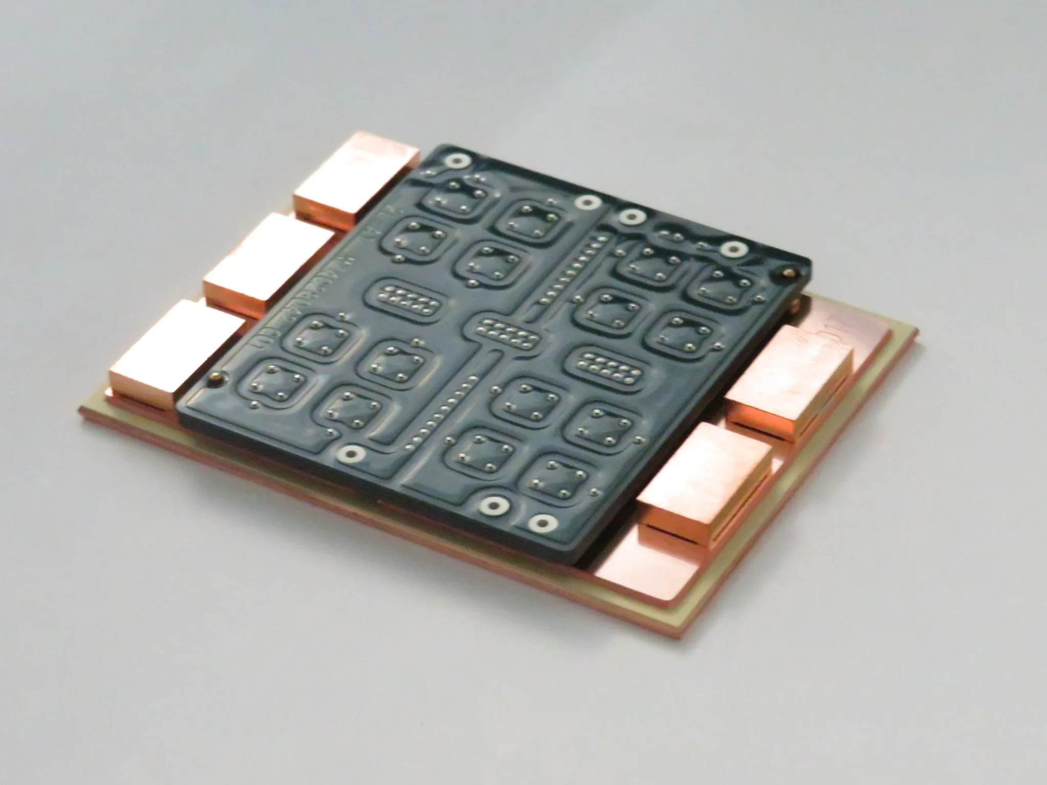
A package with a 3D wiring structure. The black part is the printed circuit board.
-
-
Electrified vehicles are expected to become more widespread with the medium- to long-term shift to decarbonization. Those powertrains are composed of motor and inverter, which draws power from a battery to rotate the motor. To overcome the challenges of improving driving range and expanding interior space, it is necessary to miniaturize the Electrified powertrain and improve its performance.
It is also necessary to miniaturize the power semiconductor modules applied on the inverters and to improve the output and efficiency. Therefore, there is a growing trend of adopting SiC-MOSFETs, which significantly reduce losses compared to conventional ones. Meanwhile, to maximize the performance of SiC, smaller package and lower power loss are required. The package connecting power chips electrically, forms circuits, and then encapsulates them with resin to protect them from vibrations and dust in the air.
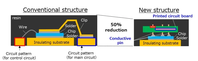
The recently developed 3D wiring structure is a packaging technology for miniaturization and lowering power loss. Conventionally, wires and clips were used to connect the chips on the insulated substrate (outlined in red and blue in the figure below). In the new structure, the wiring has been replaced with a printed circuit board, which is connected in three dimensions by using conductive pins press-fitted into the board. This has reduced the volume of the product by approximately 50% compared to the conventional product.
In addition, optimizing the current path by 3D wiring structure has successfully reduced the parasitic inductance of the internal circuit, approximately 70% less than our conventional product, and leading to an approximately 50% reduction in switching loss.
Furthermore, the structure by wiring with conductive pins can reduce the area of the chip joint compared to the conventional one, and relieving the strain by the thermal deformation on its joint is able to improve approximately five times lifetime of the joint.
This technology will be applied to its power semiconductor modules in FY2026.
<Inquiries>
Business Planning Department, Business Management Division, Semiconductors Business Group, Fuji Electric Co., Ltd.
☎ +81-3-5435-7158
-
Note:
-
Information contained within this news release is as of the time of release and is subject to change without prior notification.