Fuji Electric and Furukawa Electric to Set Up a Technology Research Association for Next Generation Power Device
June 22,2009
Furukawa Electric Co., Ltd. Fuji Electric Holdings Co., Ltd.
Aiming to be the First Association to be Approved by the Revised Research Associations for Mining and Manufacturing Technology Law in Japan
Furukawa Electric Co., Ltd (President: Masao Yoshida; Headquarters: Chiyoda-ku, Tokyo) and Fuji Electric Advanced Technology Co., Ltd. (President: Naoya Eguchi; Headquarters: Hino-shi, Tokyo), a research and development (R&D) subsidiary of Fuji Electric Holdings Co., Ltd. (President: Haruo Ito; Headquarters: Shinagawa-ku, Tokyo) announced today that the both companies would set up a technology research association for next generation power device to jointly develop gallium nitride (GaN) power devices.
Furukawa Electric has strength in basic research on GaN whereas Fuji Electric has established mass production and reliability technologies. By complementing each other with their own advantages, the both companies will strive to accelerate time-to-market for next generation power device products. Research Associations for Mining and Manufacturing Technology Law in Japan has been revised this year to enable research associations to incorporate and commercialize research achievements. Aiming to be the first association to be approved under the revised law, the both company made an application today for foundation of a technology research association for next generation power device. The technology research association is scheduled to be inaugurated in July 2009 and aims to commercialize GaN power devises in 2002
1. Objectives
(1)
Contribute to the progress of power electronics through development of GaN power devices, which help energy-saving and environmental protection
Silicon (Si) is currently used as the mainstay material for power devices. However, it is considered that it is impossible to reduce further energy loss as it has already reached the limit. Therefore, new materials such as GaN and silicon carbide (SiC) have been drawing attentions. The SiC schottky diode (SBD*1) is already available in the market but it is difficult to create a large substrate using SiC due to large costs. The GaN power device has a great potential to be used for a high-speed switching device and replace with IGBT due to its superior features such as high-voltage and low-loss. However, it has still not gone beyond research level.
In the meantime, crystal defects have significantly been reduced and device performance has considerably improved in the past several years. This enables us to prototype the high-efficiency power supplies required for switch-mode power supplies within a few years. By becoming the first to offer the prototype in the market, the Fuji Electric Group can make a great contribution to the progress of power electronics as well as make a large step toward commercialization of GaN power devices.
(2)
Accelerate development of next generation products by leveraging the both companies' respective core technologies
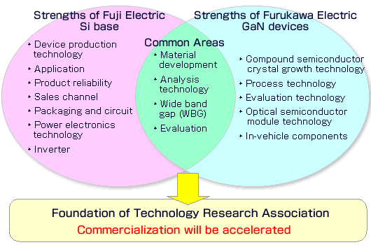
Furukawa Electric has made significant achievements in the GaN power device field and attracted the world's attention as a result of its continuous R&D efforts for transistors and diodes using GaN (see Figure 1.)
Fuji Electric Advanced Technology Co., Ltd., an R&D subsidiary of the Fuji Electric Group, has core technologies in the power device development (see Figure 2.) and the R&D of power device application products, including inverters and power supplies, as well as many researchers and engineers who are engaged in different device designs and processes.
The collaboration announced today enables the two companies to tap into each others strengths to accelerate development of practical power devices (see Figure 3.) In addition, by sharing R&D costs between the two companies, large R&D projects will be made possible, reducing time-to-market.
Figure 3. Competitive strengths and synergy of the both companies
(3)
Incorporate research achievements in accordance with the revised Research Associations for Mining and Manufacturing Technology Law in Japan
The Research Associations for Mining and Manufacturing Technology Law in Japan was established in 1961 to enhance an efficient use of R&D resources. Since then, many private companies and other organizations have set up technology research associations for joint R&D projects in accordance with the law.
In April 30, 2009, the law was revised so that technology research associations can be changed to corporations to commercialize research achievements. In addition, an application for foundation of a technology research association is now allowed to make upon agreement of two companies. This will simplify and facilitate the application procedure. Against this backdrop, the both companies made an application, aiming to be the first association to be approved under the revised law.
2. Target Markets
Since devices can be created on the Si if GaN is used, GaN has a more advantage in terms of costs than SiC, in which the substrate cost is not expected to lower soon. Therefore the device will target the low- and middle-voltage markets, where tougher cost requirements must be met. Also, GaN power devices are green devices which help achieve a low carbon society, with energy loss of more than one-tenth of that of Si devices. This green feature will fit for the hybrid and electric vehicle markets as well as the industrial power supply and general-purpose inverter markets. New opportunities are also expected by leveraging high-speed switching feature of GaN. Further discussions will be made within the technology research association on this matter.
3. Purpose and Outline of the Technology Research Association
(1)
Purpose
This association aims to develop and commercialize SBDs and metal oxide semiconductor field effect transistors (MOSFETs) within 3 years.
(2)
Name
The name of the association will be Next Generation Power Device Technology Research Association.
(3)
Location
The association will be set up within the Yokohama research center of Furukawa Electric for the first year.
(4)
Contribution
The association will be run for ¥ 800 million for the first year.
(5)
Organization
Hisao Shigekane, Director of Fuji Electric Holdings, will be appointed as the director of the association and Kazunori Nakamura, Corporate Senior Vice President of Furukawa Electric will be appointed as the executive director. 22 researchers will be assigned for the first year.
4. Details of R&D Activities
(1)
Development of Epitaxial Technology
Aiming for commercialization for SBDs and MOSFETs, the both companies will develop technology for growing high-quality GaN crystal on the Si substrate, in which a reduction in cost is expected. Specifically, the both companies will strive to reduce crystal defects and crystalline stress to improve quality by using epitaxial crystal growth technology*2 and controlling deposition conditions of buffer layer on the Si substrate.
(2)
Development of SBD and MOSFET Devices
The both companies will develop the device structures and the process technology required to create the low-loss diodes and MOSFETs applicable to switch-mode power supplies. The both companies will not only study device structures but also study and evaluate reliability of device implementation structures. Based on the result, design samples and engineering samples will be created to be evaluated publicly.
(3)
Study for Commercialization
Considering features of GaN SBDs and MOSFETs as power semiconductor device, the both companies will seek for and identify applicable markets where GaN devices have advantages over existing Si or SiC devices. The both companies will also clarify device specifications and costs required in the applicable markets and incorporate them into the development goal as well as propose what kind of businesses can be developed.
5. R&D Schedule of the Technology Research Association
Fiscal 2009:
Proof-of-principle prototyping of 600V withstand-pressure SBD and identification of process issues
Review and proof-of-principle prototyping of MOSFET structure
Fiscal 2010:
Production of design samples
Fiscal 2012:
Production of engineering samples and discussion on volume production lines
*1
SBD: Schottky diode
A Schottky diode uses a metal-semiconductor junction as a Schottky barrier (instead of a semiconductor-semiconductor junction as in conventional diodes). This Schottky barrier results in both very fast switching times and low forward voltage drop compared to the p-n junction diode.
*2
Epitaxial crystal growth
It is one of membrane crystal growth technologies, where crystal is grown on and aligned to the surface of the crystal substrate. In GaN power devices, epitaxial crystal is grown on the buffer layer placed on the Si substrate.